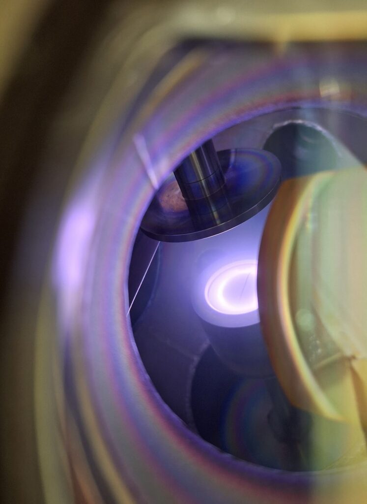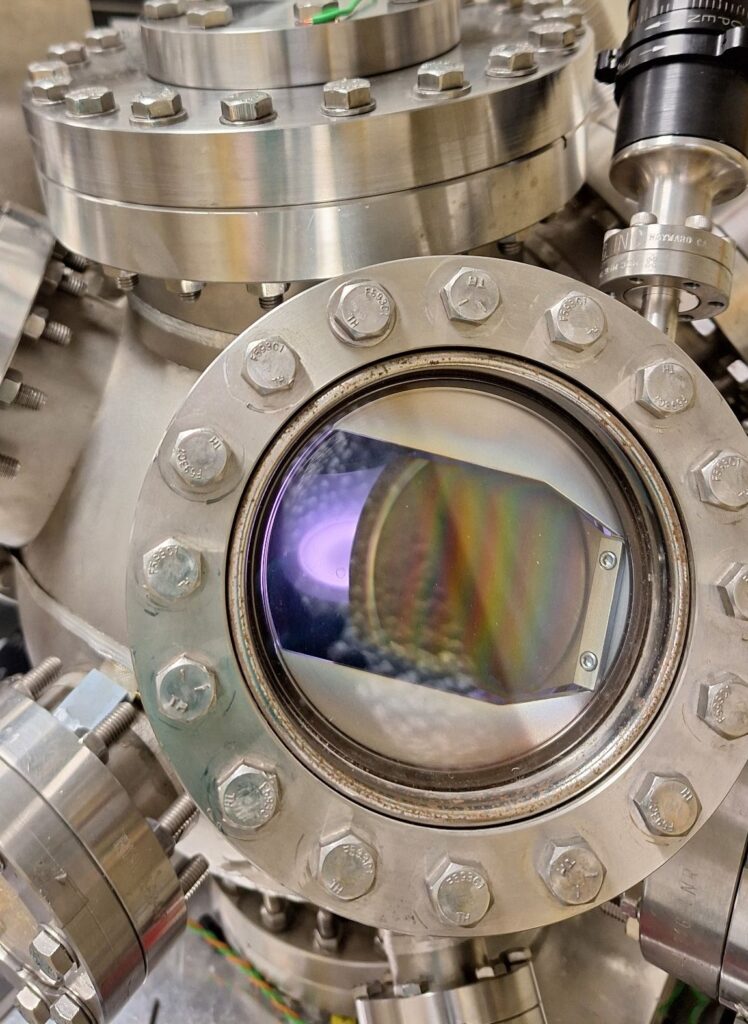

We are thrilled to announce the installation of our new home-made sputtering deposition machine, designed exclusively for the deposition of Ga2O3 thin films! This chamber was developed as part of our scientific project focused on the advancement of Ga2O3-based field-effect transistors for biological applications. Our Wide BandGap Semiconductors group is committed to pioneering research in the fields of photonics, electronics, and optoelectronics using wide bandgap materials.